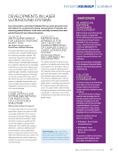
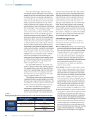
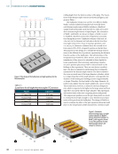
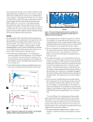
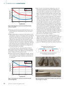
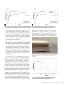
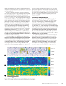
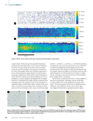
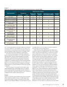
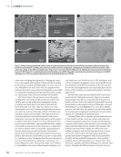
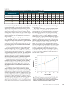
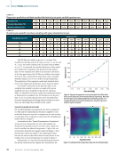
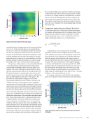
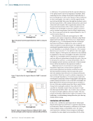
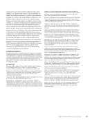
ultrasonic waves within a sample. Laser ultrasonic methods are suitable to perform in situ or in the online inspection of parts with very complex geometry in a high-temperature environment (Lévesque et al. 2016). Recent progress in laser induced phased arrays (LIPA) (Pieris et al. 2020) has demonstrated that LIPA is a viable remote, nondestructive, UT technique capable of being implemented as part of an online inspection of AM as seen in Figure 5. It is worth noting that the LIPA system described by Pieris et al. (2020) had some difficulty sizing the defects, but that the positional accuracy was quite good. This issue of sizing may be improved by either optimizing the shear wave frequency or through more sophisticated data processing, perhaps through models that can handle multiple modalities. Spatially resolved acoustic spectroscopy (SRAS) is an acoustic technique that uses surface acoustic waves to map the grain structure of a material (Smith et al. 2014), includ- ing local crystallographic orientation and texture. The use of surface acoustic waves has been correlated with build quality of SLM parts (Smith et al. 2016b). In some respects, SRAS results provide a high spatial assessment of the materi- al’s state, and thus can serve as so-called ground truth when other (cheaper) NDE methods are used and, potentially, fused. Figure 6 provides an example of SRAS grain size and orienta- tion measurement. Acoustic Emission Testing Acoustic emission testing (AE) is an NDE method that measures the elastic energy released in the form of acoustic waves in materials that undergo some type of change (such as plastic deformation, cracking, or rupture) (Ida and Meyendorf 2019). Passive monitoring of acoustic signatures has been performed for a directed energy process, showing variations in acoustic emission signatures that correlate with varying process parameters. Because the technique is passive, little modification is required for integration with AM systems, while exhibiting good sensitivity to crack-like events (Koester et al. 2018). One of the exciting demonstrations of the appli- cation of UT to AM involves the assessment of a type of hybrid AM, where the material state has been tuned through the nonuniform application of a secondary peening process (Sotelo et al. 2021). This work shows that UT can be used to spatially assess differences in the material state, providing a promising pathway for future efforts where the composi- tion and material state may change within a single unitized structure. The attenuation map shown in Figures 7a and 7b suggests that the microstructure of these samples is mostly homogeneous, despite the known heterogeneity introduced by the AM process, and Figure 7c exhibits a pronounced cyclic behavior, which is primarily attributed to microstruc- tural changes imparted by the hybrid process. Electromagnetic Testing From low frequency to high frequency, this family of NDE techniques comprises alternative current potential drop (ACPD), eddy current testing (ECT), and microwave and millimeter wave techniques as well as Terahertz measurement technology. ECT is arguably the most promising technique of these four candidates for metal powder–based AM processes because it offers a noncontact and high-speed way to inspect surface and near-surface features of samples under test. Due to the skin effect that depends on the working frequency and the material’s electrical properties, it is very difficult for ECT to probe deep features (for example, 20 mm deep cracks) for fer- romagnetic materials. However, such depth measurements are possible for nonferromagnetic materials if a special coil design is used (Janousek et al. 2005). Traditional coil-based ECT systems have been proven applicable for surface and near- surface (depth = 1.2 mm, minimum length = 0.2 mm, material = Ti64) cracks in an AM manufacturing environment (Du et al. 2018). Advancement in magnetometer technology has helped to improve the performance of ECT in terms of minimum detectable defect size. A heterodyne ECT system based on a magnetoresistive sensor has been shown to be able to detect surface defects in the order of 100 μm (Ehlers et al. 2020), as seen in Figure 8. Eddy current in array form (ECA) has recently been used for AM process monitoring due to its superior performance compared to its single-channel counterparts. ECA techniques can detect discontinuities, surface irregularities, and undesir- able metallurgical phase transformations in magnetic and non- magnetic conductive materials additively manufactured using laser powder bed fusion (Todorov et al. 2018). Electromagnetic techniques in general are sensitive to bulk electrical properties of the samples under testing, Scan axis (mm) Build direction (+z) 2.4 2.2 2 4 2 0 0 5 10 15 20 2.2 2 1.8 4 2 0 0 5 10 15 20 2.2 2 1.8 4 2 0 0 5 10 15 Figure 7. Attenuation, α (Np/m), maps for: (a) wrought (b) AM and (c) hybrid AM samples. Note the differences in scale (reprinted with permission from Sotelo et al. [2021]). A P R I L 2 0 2 2 • M A T E R I A L S E V A L U A T I O N 55 Index axis (mm) Index axis (mm) Index axis (mm)

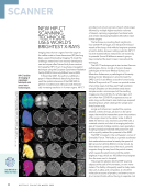
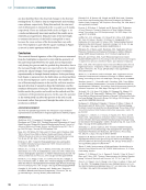
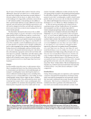
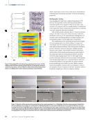
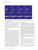
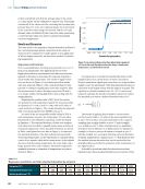
which, based upon current work, makes them unsuitable for evaluating microstructural anomalies as well as mechanical properties. Radiographic Testing X-ray imaging (2D) and X-ray computed tomography (CT) (3D) are very powerful tools for detecting internal defects embedded inside of the sample for both in situ and ex situ scenarios. The output results are usually intuitive visualizations of the inspected volume, making data interpretation a relatively easy task compared with other modalities. With its high spatial resolution, micro CT has been demon- strated to be able to detect low volume fractions of porosity (du Plessis et al. 2015), LOF, and inclusions, making micro CT an ideal tool for developing AM process improvements and ensuring the quality of certain high-value components. The combination of the resolution and penetration depth of X-ray imaging makes it an ideal technique to image and scientifically study the subsurface physical phenomena associ- ated with the dynamic behavior of the laser powder bed fusion process. Subsurface melt-pool dynamics, including keyhole dynamics and collapse, vapor bubble formation and motion, and the effect of laser turnaround parameters on the depth of the molten pool and associated generated defects can all be observed using imaging using X-rays (or other high-energy particle techniques, such as neutron or protons), which permits some fundamental studies to be conducted that are otherwise exceptionally difficult, if not impossible, for surface-sensitive process monitoring tools (Calta et al. 2019). Figure 9 demon- strates the possibility of using in situ X-ray imaging to observe the dynamics of pore formation at the laser turnpoint, which is helpful for designing an effective mitigation strategy. x (mm) V (V) –5.5 –5 0 1 2 3 4 9 8 7 6 5 4 3 2 1 0 –4.8 –4.9 –5 –5.1 –5.2 –5.3 –5.4 –5.5 Figure 8. Heterodyne ECT system based on a magnetoresistive sensor: (a) CAD drawing of desired defect geometry (depth 200 μm) (b) microscopic picture of artificial surface defects and (c) ET data of artificial surface defects (reused from Ehlers et al. [2020] under Creative Commons Attribution License [CC BY]). 500 μm Voids Turn point Turn point Track Surface depression Powder Side-on Top-down Figure 9. Illustration of the experimental geometry for laser turn point experiments: (a–c) illustration of the laser turnaround point studied here (d–f) time difference X-ray images of a turnaround in Ti-6Al-4V performed at a laser power of 200 W and set scan speed of 1000 mm/s (d) laser scanning from the left to right with spatter and powder above a melt depression due to vapor recoil below (e) laser entering the turn point region and the vapor depression digs deep into the substrate (f) laser moving right to left after the turnaround. Keyhole voids at the turnaround location are highlighted in red. (Figure is reused from Calta et al. [2019] under Creative Commons Attribution License [CC BY].) ME | AMNDEOVERVIEW 56 M A T E R I A L S E V A L U A T I O N • A P R I L 2 0 2 2 y (mm) 2 mm 2 mm 2 mm 2 mm 200 μm 150 μm 100 μm 50 μm V (V)
ASNT grants non-exclusive, non-transferable license of this material to  .
All rights reserved. © ASNT 2026. To report unauthorized use, contact: customersupport@asnt.org